|
The PCB’s are fabricated by using modern small capacity technological processes installed in production laboratories of the department:
|
 |
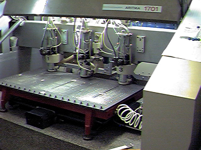
CNC 3-spindle drilling machine |
|
electroless/electrolytic plating line (with manual manipulation) |
|
brushing and cleaning machines |
|
dry photoresist hot roll laminator |
|
solder mask vacuum laminator |
|
permanganate desmear process |
|
exposure unit |
 |
developing, etching and stripping lines |
 |
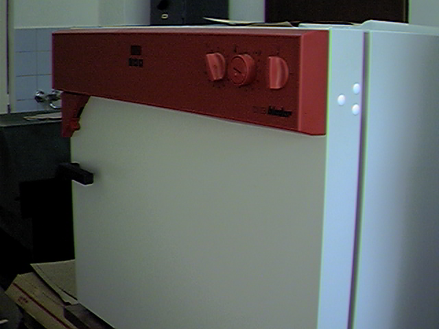
drying ovens |
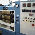 |
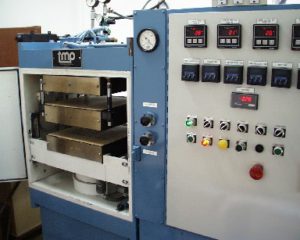
multilayer press |
|
electrolytic gold plating equipment |
|
lead-free HASL |
 |
PCB shape is finished by 1-spindle CNC routing machine or by optically controlled manually operated guillotine |
|
Ecological safety is maintained by waste water neutralisation and disposal station. |
| |
| Basic Technical Parameters |
| Final PCB size: |
max. 400 x 400 mm |
| Standard thickness (up to 8-layer PCB): |
1,5 mm |
| Basic material: |
FR-4 |
| Cu thickness: |
18 or 35 um (option: 70, 9 or 5 um) |
| Drill diameter: |
min. 0,5 mm (optionally 0,3 mm) |
| Basic prices |
| Single sided PCB |
3.5 EUR/dm2 |
| Double sided PCB (line/space density to 0.3 mm) |
8.1 EUR/dm2 |
| 4-layer PCB |
14.3 EUR/dm2 |
| 6-layer PCB |
17.8 EUR/dm2 |
| 8-layer PCB |
22.0 EUR/dm2 |
Optional technological processes (HAL, soldermask, gold plating, component screening, shaping by routing machine) are extra accounted.
Quantity discount: 10 % for more than 20 pcs. |
| |
| Contact Person |
| Head of production technology: Ing. Ivan Bešina, Phone: +421 2 5941 1113
|
|
 PCB laboratory