 Laboratory for EBL and micro-technology Laboratory for EBL and micro-technology
The R&D infrastructure of Electron beam lithography Department is divided into the following laboratories:
1. Laboratory of electron-beam lithography
2. Laboratory of photolithography
3. Laboratory of thin films preparation
4. Laboratory of plasmatic etching
5. Laboratory of optical microscopy
6. Laboratory of the evaluation, measurement and analysis of structures
7. Chemical laboratory for the work with acids, hydroxides, polymers, polyimides and chemical solutions
8. Laboratory for the finalization of chips
The base of this R&D infrastructure are air-conditioned cleanrooms in the building of our Institute. They can be divided into three categories:
1. Clean laboratory rooms with air conditioning with the area of 90 m2.
2. The clean rooms with powerful air-conditioning with minimal purity class 1000 and temperature stability of ±3°Cand the area of 65 m2 (total area in this part are 112 m2).
3. The clean rooms with powerful air-conditioning with minimal purity class 1000 and temperature stabilityof ±0,5°Cand the area of 65 m2.
Equipment in Laboratories is listed:
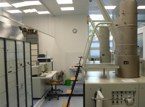
• Among the unique and key equipment of the R&D infrastructure of the applicant belong 2 electron-beam pattern generators (lithographs) with variable beam cross-section of the electron beam: the electron-beam pattern generator ZBA 21S with energy of electrons 20 keV (Vistec-Leica Microsystems Lithography) which allows preparation of the structures in submicrometer range of dimensions (minimal reproducible dimension 400 nm) on the substrates with diameter of up to 15 cm; electron-beam pattern generator ZBA 23 with energy of electrons 40 keV (Vistec-Leica Microsystems Lithography) which anables preparation of the samples in submicrometer range of dimensions (minimal reproducible dimension 200 nm) on the substrates with diameter of up to 18 cm.
• Other infrastructure of the Electron beam lithography Department according to the following list enables the evaluation and analysis of lithographic structures, preparation of thin films, photolithography, thickness measurement of thin films, processes with polymers, polyimides, chemicals and solutions and preparation of devices for measurements:
Microscopy methods:scanning electron microscope with autoemission cathode S-800 (Hitachi), 2 nm resolution. Optical microscopes.
Photolithographic equipment:MJB3 (KarlSuss), 2 micrometers resolution.
Thin films deposition:the equipment for magnetron sputtering SCM 600 (Alcatel) and the equipment for evaporation using electron gun (with a planetary system) (VEB HochvakuumDresden).
Correction of defectsin thin chromium layers on the photomasks: the equipment with a pulse powerful laser beam NEC YL451 (NEC).
Thin films thickness measurement: profilometer Alphastep (Tencor Instruments), resolution of several nanometers.
Processes with resists and polyimides:cleaning (Ultratech), spin coating (Convac 1001G, Convac 1001 GS ver. 8531), wet chemical etching in acids, hydroxides and solutions, production of deionisedwater (W.Werner).
Equipment for the chips finalization:diamond saw, chips contacting (VEB Elektromat).
• Further equipment required for the research specialization of the Department of EBL is supplied withing the cooperation with other reserach facilities. Plasmatic etching of the structures using reactive ion etching with ECR source (ECR RIE) is supplied by the cooperation with ElÚ SAS (Institute of Electrical Engineering SAS)and plasmatic etching of the structures using reactive etching with ICP source (ICP RIE) is supplied by the cooperation with FEI STU (Faculty of Electrical Engineering STU). Supplementary scanning electron microscopy is supplied by the cooperation with ElÚ SAS on the Quanta FEG250 (FEI) equipment.
|